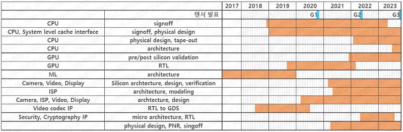
So according to this LinkedIn research, the Tensor IP blocks were designed by:
- CPU (frontend): Samsung S.LSI for all
- CPU (backend): Google for all
- GPU (frontend+backend): Samsung S.LSI for OG Tensor, Google for G2-G3
- NPU/TPU (frontend+backend): Google for all
- Multimedia IP (ISP, Video Encode/Decode, Display) (frontend+backend): for the OG Tensor Google only designed the Video Encode/Decode, but starting with the G2 Google also designed the ISP and Display blocks
Seems like Google is progressively getting more involved in the design process, which makes sense if the rumours of going TSMC for the Pixel 10 are true
Seems like Google is progressively getting more involved in the design process, which makes sense if the rumours of going TSMC for the Pixel 10 are true
That might be true, but the Tensor G3 has unexpectedly worse CPU efficiency than it’s predecessors according to GoldenReviewers testing, despite the better processing node (SF4/4LPP second gen 4Nm node), supposedly same amount of cache (according to XDA) and with cores that are two generations newer. The SPEC results (will add them later) of the big X3 core are worse than the ones of the X1 core inside the SD888, which also clock at a similar clock speed.
My current theory is that there is something flawed about the Tensor G3’s CPU design and the problem doesn’t stem from the processing node, which most people seem to conclude to.
For CPU design, there’s no change from OG to G3. Samsung S.LSI has done all the frontend design and Google has done all the backend design
My current theory is that there is something flawed about the Tensor G3’s CPU design and the problem doesn’t stem from the processing node, which most people seem to conclude to
The main reason GoldenReviewers’ testing shows worse efficiency is because the subscore for 462.libquantum is extremely low, only 25.05, when it should be >150
It’s possibly a design flaw in hardware
But it could also be a bug in the scheduler/DVFS/something else in the BSP
Why didnt Samsung get feedback from Google in the CPU design development process? I’m guessing Google wanted a specific function in the CPU and Samsung delivered it with a flaw.
It seems there is a chronic problem at Samsung with soc/fab development my guess is that people underestimate how godly hard it is to build a soc/fab company from scratch. It is not easy to make the brains of a computer. Ram/SSD/display is child’s play compared to an soc.
If I was the chairman at Samsung, I would get talent from across the world for the Fab and exynos division.
Sigh…they should just get an American to develop an exynos chip and branch it off.
Nothing to be ashamed of. Apple still has Samsung IP blocks in their M series SoCs from back when they used to rely on Samsung the same way Google does now.