- 이전 포스팅에서 텐서G3 성능 문제를 다뤘는데 구글 텐서 설계 주체는 가설에 영향을 크게 주는 요소인데 너무 대충다룬 느낌이었음. ( 구글 텐서G3 CPU 성능 이슈 분석. (Tensor G3, S5P9865) ) 그래서 이를 명확히 하고자 추가 정보를 체크해봄. - 확인 가능한 정보. (공식 표기는 텐서, 텐서G2, 텐서G3지만 여기서는 텐서1,2,3로 표기하겠음.) 삼성 텐서1,2,3 시스템 레벨 캐시 아키텍처, 마이크로 아키텍처(CPU?), RTL 디자인. 텐서3 인터커넥트, 메모리 서브 시스템 아키텍처. CPU를 포함한 주요 부분 프론트 엔드를 작업한 것으로 추정. 구글 pre/post silicon validation 구글 텐서 GPU RTL 디자인. 구글 텐서1,2,3 CPU, 시스템 레벨..
For CPU design, there’s no change from OG to G3. Samsung S.LSI has done all the frontend design and Google has done all the backend design
My current theory is that there is something flawed about the Tensor G3’s CPU design and the problem doesn’t stem from the processing node, which most people seem to conclude to
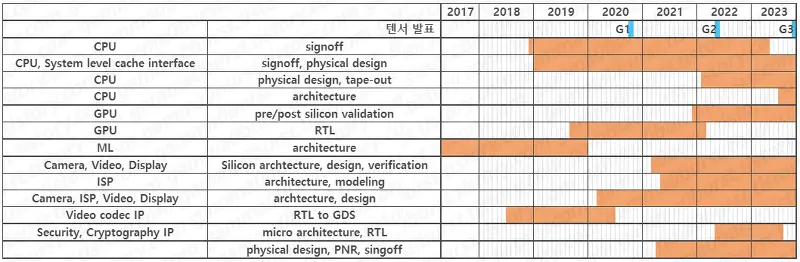
For CPU design, there’s no change from OG to G3. Samsung S.LSI has done all the frontend design and Google has done all the backend design
The main reason GoldenReviewers’ testing shows worse efficiency is because the subscore for 462.libquantum is extremely low, only 25.05, when it should be >150
It’s possibly a design flaw in hardware
But it could also be a bug in the scheduler/DVFS/something else in the BSP